9.3.2.2 Full-wave Rectification

  1. Figure above shows a circuit to produce full-wave rectification. 
  2. Using an ingenious arrangement of diodes, called a bridge rectifier, this reverses the negative half of each a.c. cycle, instead of just blocking it. 
  3. The result is that current always flows in the same direction through the load, no matter which way it leaves the supply. 
  4. Combine a transformer (to reduce mains voltage) with a bridge rectifier and a smoothing capacitor, and you have a mains-operated d.c. power supply - as used in radios, instead of batteries.
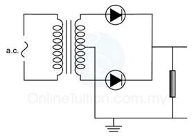
  5. Another method of full wave rectification is arrange two diode to the output of a transformer as show below. A similar result will be produced.

Smoothing


  1. In the circuit above, the `one-way' direct current flows in a series of surges with brief periods of zero current in between. 
  2. These surges can be partly smoothed out by connecting a large capacitor across the load.
  3. The capacitor charges up when current flows from the diode, then discharges through the load when the current from the diode is zero. 
  4. Smoothed in this way, the current through the load is similar to the steady direct current which would flow from a battery. 


9.3.2.1 Half-wave Rectification

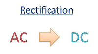
  1. Diodes are also known as rectifiers. They can be used to change a.c. into d.c., a process called rectification.
  2. A simple rectification circuit is shown in figure below.
  3. The final waveform on the screen is the positive half only of the original a.c. waveform - hence the term 'half-wave' rectification.

Half-wave rectification: the negative part of the current is prevented from passing.


9.3.1 Semiconductor Diodes

The p-n junction

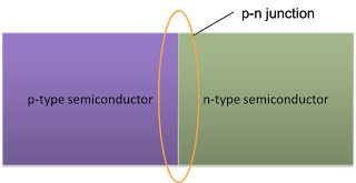
  1. We can produce a single crystal with p-type semiconductor on one side and n-type on the other side as shown in figure above.
  2. The border where the p-type and the n-type region meet is called the p-n junction.

Depletion Layer and Junction Voltage

  1. At the p-n junction, electrons from the n-type semiconductor will be attracted to the holes in the p-type semiconductor.
  2. As a result, the holes and the electrons at the p-n junction disappear, forming a layer called “depletion layer”.
  3. At the same time, the p-type semiconductor becomes more negative whereas the n-type semiconductor becomes more positive.
  4. This will result a potential difference across the p-n junction. This potential difference is called the junction voltage (or the barrier voltage).
  5. The junction voltage will prevent the charge carrier from flowing across the depletion layer.

Forward Bias And Reverse Bias

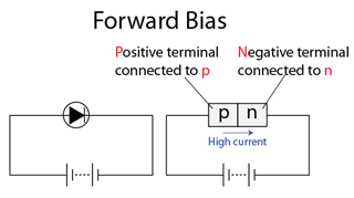
(figure 1)
  1. The figure above shows a dc source across a diode. The negative source terminal is connected to the n-type material, and the positive terminal is connected to the p-type material. 
  2. This connection Figure is called forward bias.
  3. Current flows easily in a forward-biased silicon diode.
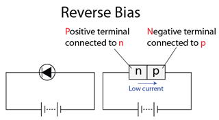
    (Figure 2)
  4. Turn the dc source around and you reverse-bias the diode as shown in Figure 2. 
  5. This time, the negative battery terminal is connected to the p side, and the positive battery terminal to the n side. This connection is called reverse bias.

Depletion Layer Widens

  1. The negative battery terminal attracts the holes, and the positive battery terminal attracts the free electrons. Because of this, holes and free electrons flow away from the junction. Therefore, the depletion layer gets wider.


9.2.2.2 P-type Semiconductor

  1. A p-type semiconductor can be produced by doped some trivalent atoms into a semiconductor.
  2. Trivalent atom is atom has only three valence electrons. Examples include aluminum, boron, and gallium.
  3. Figure above shows an aluminium atom (which is trivalent ) in the center, surrounded by four silicon atoms.
  4. We can see that, the trivalent atom form 4 covalent bonds with the silicon atoms around. Since the trivalent atom has only three valence electrons and each neighbour shares one electron, only seven electrons are in the valence orbit..
  5. This means a hole exists in the valence orbit of each trivalent atom. A trivalent tom is also called an acceptor atom because each hole it contributes can accept a free electron.
  6. The more trivalent impurity that is added, the more holes in the semiconductor, and hence the greater the conductivity of the semiconductor.
  7. Some free electrons will also formed in the semiconductor when some electrons are promoted to shell with higher energy level.
  8. The holes outnumber the free electrons, hence they are called the majority carrier and the free electrons are called the minority carriers.
  9. Since the positive charge carrier (the holes) outnumber the negative charge carrier (the free electrons), the semiconductor is called a p-type semiconductor, where the p stands for positive. 


p-type semiconductor n-type semiconductor
Doping Material Trivalent:
aluminum, boron, and gallium
Pentavalent:
antimony, and phosphorus
Role of doping material Atom receiver Atom donor
Majority Charge Carrier Holes Free electrons
Minority Charge Carrier Free electrons Holes


9.2.2.1 N-type Semiconductor

  1. n-type semiconductor can be produced by doped some pentavalent atoms into a semiconductor.
  2. Pentavalence atoms are atoms that have 5 electrons in the valence shell. Examples of pentavalent atoms include, antimony, and phosphorus.
  3. Figure above shows how the silicon crystal appears after doped with a phosphorous atom, which is pentavalence.
  4. We can see that, the pentavalence atom form 4 covalent bonds with the silicon atoms around. Since a pentavalence atom has 5 electrons, there is an extra electron left over and it is a free electron.
  5. Each pentavalent in the silicon crystal produces one free electron. Therefore, the pentavalence atom is called the donour.
  6. The more pentavalence impurity that is added, the more free electrons in the semiconductor, and hence the greater the conductivity of the semiconductor.
  7. Some holes will also formed in the semiconductor when some electrons are promoted to shell with higher energy level.
  8. The free electrons outnumber the holes, hence they are called the majority carrier and the holes are called the minority carriers.
  9. Since the negative charge carrier (the electrons) outnumber the positive charge carrier (the holes), the semiconductor is called an n-type semiconductor, where the n stands for negative. 


9.2.2 Doping of Semiconductors

  1. One way to increase the conductivity of a semiconductor is by doping
  2. Doping is a process of adding a small amount of impurities to a semiconductor.
  3. The impurities added to the semiconductor are called dopants.
  4. By adding impurity atoms to a conductor can increase its electrical conductivity
  5. There are two types of semiconductor depending on the type of impurities doped, namely
    1. the n-type semiconductor
    2. the p-type semiconductor


9.2.1 Semiconductors

  1. Semiconductor is a class of crystalline solid with conductivity between a conductor and an insulator.
  2. Example of semiconductors are:
    1. Silicon
    2. Germanium
    3. Boron
    4. Tellurium
    5. Selenium

The Silicon Crystal


  1. The typical example of semiconductor is silicon.
  2. Silicon has 4 valence electrons. Each of these 4 electrons are shared with another 4 silicon atoms to form 4 pairs of covalent bond, as shown in the diagram above.
  3. The bonded valence electrons are not free to move. Therefore silicon is not a good conductor at room temperature.
  4. At room temperature, a silicon crystal acts approximately like an insulator because only a few free electrons and holes are presence.

Free Electron and Hole


  1. If a bonded electron absorbs heat energy from the surrounding, it may be promoted to higher energy level.
  2. These electrons are free to move when they are at a higher energy level.
  3. If an electron is promoted to higher level, a vacancy is left in the valence shell, and it is called a hole.
  4. A hole has the tendency to pull electrons. Therefore a hole is assumed carries positive charge.
  5. Both of the free electrons and the holes can help to conduct electric current.
  6. Therefore, with the presence of the free electrons and holes, the conductivity of a semiconductor is higher than an insulator.

Resistance Change Due to Temperature Change

  1. As the temperature increases, more and more electrons are getting promoted to become free electrons and at the same time creating more and more holes. Therefore the conductivity of a semiconductor increases as the temperature increases.
  2. The graph below shows the resistivity change of a conductor and semiconductor against the temperature. The resistance of a semiconductor decreases as the temperature increases.

Flows of Free Electrons and Holes

  1. We have learned that, there are 2 types of charge carrier in a semiconductor, the free electrons and the holes.
  2. The free electrons carry negative charge whereas the holes carry positive charge.
  3. If a potential difference is applied to a semiconductor, the electrons and holes will start to flow.
  4. The electrons will flow to the negative terminal whereas the holes will flow to the positive terminal.
  5. Video below explain how the free electrons and holes flow in an electric field.


9.1.5 Uses of the Cathode Ray Oscilloscope

In a laboratory, a cathode ray oscilloscope can used to

  1. display different types of wave form. 
  2. measure short time interval
  3. measure potential difference (as a voltmeter)

Displaying Wave Forms

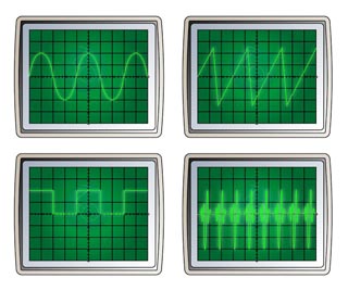
  1. A cathode ray oscilloscope can be used to display different types of waveform by connecting a power supply to the Y-input. 
  2. Figure below shows a few types of waveform displays on an oscilloscope.
Click on the links below for discussion about measuring short time interval and measuring potential difference
  1. Measuring Short Time Interval
  2. Measuring Potential Difference

Measuring Potential Difference

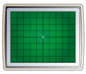
  1. In order to measure the potential difference, we need to move the bright spot to the centre before the Y-input is connected to any circuit.

  2. We also need to set the Y-gain. However, this can be adjusted later so that the signal can be fully displayed on the screen.
  3. The potential to be measured is then applied to the Y-plates via the Y-input terminals. 

Measuring Potential Difference of a Direct Current

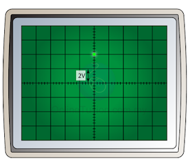
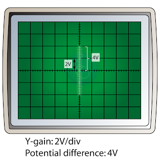
  1. The time-base is switched off. When a potential difference is applied to the Y-input, an electric field is set up between the plates. This will deflect the cathode ray either up or down.
  2. The deflection of the electron beam by an electric field is proportional to the voltage applied. The reading of the voltage can be determined by referring to the Y-gain.
  3. For example, in the figure above, if the Y-gain is set to 2V per division (2V/div), then the reading of the potential difference is 4V.
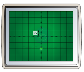
  4. If the terminal of the direct current is inverted, the bright spot will be deflected to the opposite side, as shown in the diagram below. The reading of the potential difference will remain the same (4V).

Effect of the Y-gain

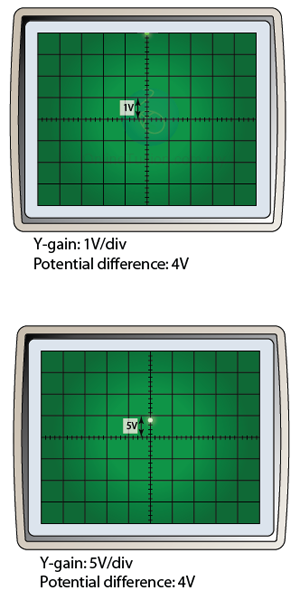
Figure below shows the display of the CRO when the Y-gain is set to 1V/div and 5V/div respectively for a potential difference of 4V.
Effect of the Time Base

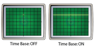
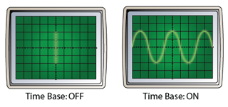
  1. The time base move the bright spot across the screen at a constant speed.
  2. Usually, the speed is very high. As a result, we are not able to see the motion of the bright spot, but a straight line across the screen.
  3. Figure below shows the display of a CRO when the time base is ON and OFF.

Measuring Potential Difference of an Alternating Current

  1. If an alternating current is connected to the Y-input, a changing potential difference will be applied between the Y-plates.
  2. The changing potential difference will move the bright spot up and down continuously.
  3. As a result, vertical straight line will form on the screen of the CRO. The reading of the potential difference can be determined by referring to the Y-gain.
  4. For example, for the diagram above, if the Y-gain is set to 2V/div, then the maximum potential difference (peak voltage) is 4V.

Effect of the Time Base

  1. If the time base is switched on, it will move the bright spot across the screen horizontally.
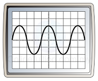
  2. The result of the vertical motion caused by the Y-plate and the horizontal motion caused by the time base is a sinusoidal wave form.
  3. Diagram below shows the CRO display when the time base is on and off.


Measuring Short Time Interval

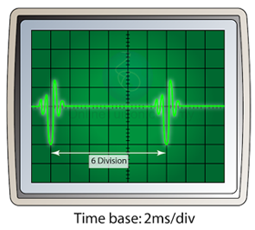
  1. A cathode ray oscilloscope can be used to determined the time interval between 2 pulses, even though the time interval is very small.
  2. Figure above shows 2 pulses on the screen of a cathode ray oscilloscope.
  3. If the time base is set to 2 ms/div, the time interval between the 2 pulses can be calculated as follow:
t = 6 x 2ms = 12 ms = 0.012s.



9.1.4 Working Principle of CRO

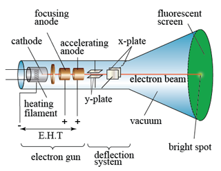
The cathode-ray oscilloscope (C.R.O.) consists of the following components:

  1. The electron gun.
  2. The deflecting plates.
  3. A fluorescent screen.

The Electron Gun

Parts of Electron Gun Function
 Filament  To heat the cathode.
 Cathode  Release electrons when heated by filament.
 Grid
  •  The grid is connected to a negative potential. The more negative this potential, the more electrons will be repelled from the grid and fewer electrons will reach the anode and the screen.
  • The number of electrons reaching the screen determines the brightness of the light. Hence, the negative potential of the grid can be used as a brightness control.
 Focusing Anode and 
  •  The other feature in the electron gun is the use of the anode.
  • The anode at positive potential accelerates the electrons and the electrons are focused into a fine beam as they pass through the anode.
 Accelerating anode


The Deflecting Plates

Part of the deflecting system Function 
 Y-plate The Y-plates will cause deflection in the vertical direction when a voltage is applied across them.
  X-plate  On the other hand, the X-plates will cause the electron beam to be deflected in the horizontal direction if a voltage is applied across them.


The Fluorescent Screen

  1. The screen is coated with a fluorescent salt, for example, zinc sulphide.
  2. When the electrons hit the screen, it will cause the salt to produce a flash of light and hence a bright spot on the screen.

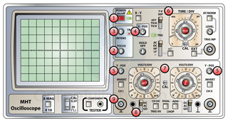
Using CRO


Function
 1. Power switch  To switch on and off of the oscilloscope
2. Focus control To control the focus of the spot on the screen.
3. Intensity control To control the brightness of the spot on the screen.
4. X-offset
5. Y-offset
Y-offset moves the whole trace vertically up and down on the screen, while X-offset moves the whole trace from side to side on the screen.
6. Time base control Whenever we switch on the time-base, we are actually applying a sawtooth voltage to the X-plates (Figure below).


* This make the electron beam sweep across the screen at a constant speed.
* By knowing the period of each cycle, T, we can then know how fast the beam is sweeping across the screen. The time-base is thus a measure of time for the oscilloscope.
7. Y gain control * the "Volts/Div." wheels amplify an input signal so that for a division a given voltage level is in valid. A "division" is a segment, a square on the screen of the oscilloscope.
* A setting of ".5" i.e. means, that the height of a single square equals a voltage of 0.5 V. An amplitude of 1 V would have a size of two divisions vertical to the abscissa.
8. d.c./a.c. switch d.c. – d.c. and a.c. voltage displayed.
a.c. – only a.c. voltage displayed.
9. X-input and Y-input Electric input connect to the X-plate and Y-plate.


Example
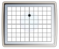
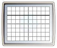
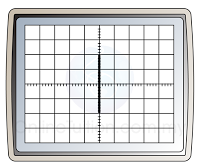
Table below shows the sample display of direct current and alternating current when the time base is switched ON and OFF.

 Direct Current (Time Base Switched Off)  Direct Current (Time Base Switched On)
 Alternating Current (Time Base Switched Off)  Alternating Current (Time Base Switched On)